WP3: Materials for Energy
WP Lead Partner: University of Montpellier
Introduction
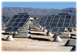 Based on some 3.1 million GWh expended in 2003, Europe is projected to consume a total electrical energy of about 3.6 million GWh by year 2020, according to a study by the International Energy Association. The implementation of novel technologies in fields such as photovoltaic cells is fundamental in order to enable the EU to meet these energy requirements in a sustainable way, lower the impact on the environment, and maintain the lead in the production chain of solar energy generation. Materials costs and availability are driving the technology towards a “third generation” of low-cost devices operating at efficiencies exceeding single-junction devices. The biggest challenge is in dramatically reducing the cost/watt of delivered solar electricity. The PVNET roadmap for Europe confirms that the priorities for III-V solar cells are to develop high efficiency (η>40%) and cost-effective cells that can operate at high sunlight flux (>500 suns) on low-cost substrates. Two approaches will be investigated in parallel to develop new materials for the next generation of CPV. In each case the architectures employed are entirely new.
Objectives:
- To improve efficiency of concentrator solar cells by exploiting intermediate band structures based on GaSb(N) quantum dots in GaAs
- To improve efficiency of Si solar cells by developing novel III-Sb/Si hybrid epitaxy for tandem cells
Partners involved in this Work Package
Collaborating partners: III-V LAB, ULANC, NOTT, Tyndall-UCC,UCA, ROME, IQE
Projects in this Work Package
Project 3.1: Growth and characterisation of dilute nitride GaSbN QD intermediate band semiconductors for high efficiency CPV solar cells.
Fellow:
Host: Lancaster University
To develop MBE growth of GaSb:N QD in GaAs for intermediate band solar cells. N (~1%) will be introduced into GaSb QD and/or GaAs barriers to alleviate strain and increase efficiency. GaAs spacer layer thickness will be studied to obtain IBSC coupling. Samples will be systematically characterised using high resolution X-ray diffraction, PL spectroscopy and AFM. Selected samples will be investigated by TEM (UCA). Prototype GaSbN QD solar cells containing stacked QD layers will be fabricated and characterised. Tyndall-UCC will provide input on band structure calculations and carrier lifetime measurements. Rome will help in understanding influence of effects on quantum efficiency variation with N incorporation and hydrogenation to investigate further improvements in efficiency. IQE will assist with concentration measurements.
Project 3.2: MBE growth of metamorphic III-Sb on Si for CPV solar cells
Fellow:
Host: University of Montpellier
To undertake MBE growth of III-V/Si templates and III-Sb heterostructures with a lattice-parameter close to InP for tandem solar cells on Si substrates. The ESR will provide InP-lattice-matched templates made of Ga0.47In0.53As/III-Sb/Si heterostructures to III-V LAB for further epitaxial overgrowth. UM2 will also grow III-Sb heterostructures on Si-junction solar cells from IQE for supply to III-V LAB. Tyndall-UCC will provide input on band structure calculations and carrier lifetime measurements. Samples will be systematically characterised using high resolution XRD, PL spectroscopy and AFM. Selected samples will be investigated by TEM (UCA).
Project 3.3: Fabrication and testing of III-V/Si tandem solar cells
Fellow:
Host: III-V Lab
GSMBE and MOVPE growth of InP-based heterostructures with bandgaps adapted for solar cells on templates provided by UM2. GSMBE growth will be intensively studied using low dopant diffusion to grow highly doped thin quaternary layers, (a key building block in fabrication of efficient tunnel junctions). These wafers and III-Sb/Si tandem heterostructures will be processed into tandem solar cells. Assessment of solar cells will be done in collaboration with IQE to enable tests under high concentration (1000 suns) where intermediate band effects are expected to bring significant improvement. Tyndall-UCC will provide calculations on band structure for tunnel-junction design. UCA will help to investigate Si/III-Sb/InP interfaces.
Project 3.4: Nanoscale characterisation of novel functional nanostructures
Fellow:
Host: University of Cadiz
To find the relation between nanostructural and functional properties, as well as growth conditions of semiconductor and plasmonic nanostructures. These include; III-V(N) QW and QD for MIR LEDs with the incorporation of plasmonic nanoparticles (ULANC), GaSb/InAsSb metamaterials (UM2) for gas sensing and III-Sb/Si for high-efficiency solar cells (UM2 & III-V LAB). Advanced electron microscopy techniques will be used, i.e. new double aberration-corrected electron microscope and an updated supercomputer, to develop new methodologies for measurements and simulations at the atom-scale. Correlation between bandstructure and nanoscale structural properties will be a priority.