WP2: Materials for Security
WP Lead Partner: University of Sheffield
Introduction
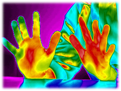 Photonics is well established as an important enabling technology for security providing the military capability for advanced warfare, including night vision, surveillance, missile guidance systems and protection against anti-terrorist threats as well as commercial an d domestic imaging and remote sensing applications. A photodiode with a following amplifier is traditionally used in sensor modules for security applications ranging from X-ray spectroscopy to long range remote sensing and 3D imaging. When the signal is extremely weak, an avalanche photodiode (APD) can provide significant sensitivity enhancement. In PROMIS, we aim to realise new metamorphic materials and detectors including avalanche photodiodes (APDs) and single photon avalanche diodes (SPADs), which will be particularly suited to mid-infrared and x-ray detection and imaging applications.
Objectives:
- To improve performance sensitivity of imaging systems by developing novel APDs and SPADs with nanometre wide avalanche regions
- To improve infrared materials using improved buffer technology
Partners involved in this Work Package
Collaborating Partners: SGENIA, ROME, ULANC, NOTT, Tyndall-UCC, IDQ, NAsP
Projects in this Work Package
Project 2.1: Nanometre wide avalanche regions for high performance single photon avalanche diodes (SPADs).
Fellow:
Host: University of Sheffield
To pioneer the design and exploitation of nm-scale avalanche regions for high performance SPADs. To ensure low leakage current, new knowledge in growth and fabrication of AlAsSb as well as optical and electrical parameters of AlAsSb will be uncovered. The breakdown voltage change is ~100 mV/K in a typical commercial InGaAs/InP SPAD. Fortunately at SHEFF Cbd ~0.95 mV/K, ~2 orders of magnitude better than the commercial SPAD, was demonstrated using an AlAsSb homojunction APD with w = 80 nm. Thin AlAsSb has also been shown to produce excess noise performance comparable to commercial Si APD, confirming reduced statistical fluctuation in the ionisation process in thin AlAsSb.
Project 2.2: Time-resolved characterisation of narrow gap semiconductors
Fellow:
Host: Tyndall-UCC
To determine radiative recombination times for InAsSb, InAs and InAsSbN/InAs/AlAsSb heterostructures of different composition and growth conditions. To find wavelength dependence of InAsSbN/InAs/AlAsSb material emitting at different energies. Wavelength, time and intensity dependence of pulsed excited emission (streak images). Time dependent streak images, excitation power dependent streak images measured and interpreted. Determination of the presence of possible defects causing the creation of non-radiative recombination channels. For Type II material, evaluation of transmission optical matrix element strength.
Project 2.3: Development and device applications of APDs for operation in photon-starved regime
Fellow:
Host: Sgenia
To exploit the properties of thin-avalanche-region APDs for the development of high-performance detector arrays operating in photon-counting mode. These APD arrays will be used to improve the maximum count rate in free-space optical communications by reducing the blocking probability due to “afterpulsing” providing imaging capabilities. The realization of APD arrays will involve the investigation of the material inhomogeneity and the underlying mechanisms behind cross-talk effects associated with interpixel coupling, as well as the design of suitable electronics to operate both the devices and arrays for the required applications (e.g. spatial filtering capabilities are of interest to mitigate the effect of background). Plasmonic and photonic crystal-like structures will be studied to add functionality in terms of spectral selectivity and optical coupling.
Project 2.4: APDs with ultra-thin avalanche region for sensitive X-ray detection
Fellow:
Host: University of Sheffield
To exploit the significantly stronger absorption efficiency of InGaAs together with a sub-50 nm avalanche region (since thin avalanche region minimises energy resolution degradation). This is a promising approach to achieve high sensitivity with shallow pixels (<6 m), leading to feasible high energy resolution high format X-ray APD imaging arrays. To show that the APD can move the signal away from the noise floor of the read-out electronics hence enhancing the sensitivity of X-ray detectors. Demonstration of soft X-ray detection using InGaAs absorption with nm-scale AlAsSb avalanche region to achieve shallow pixel with good energy resolution.