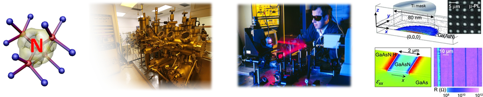
Dilute Nitrides
The aim of this project is to produce novel device-quality dilute nitride semiconductors to enable the development of photonic devices for the technologically important mid-infrared (3-5 µm) spectral range. There are extensive requirements for mid-infrared tunable diode lasers, LEDs, photodetector arrays and sensitive, high speed avalanche photodiodes (APDs) in applications including remote gas sensing, active imaging and night vision, healthcare and spectroscopy. Incorporation of small amounts of N into III-V’s causes conduction band anti-crossing leading to reduction in band gap and offers an attractive way of tailoring devices.
We shall exploit the properties of substitutional N to engineeer the band structure of InAsN(Sb) grown on GaAs substrates to enable the development of affordable high performance light sources and detectors operating at room temperature.
The specific objectives are:
- To develop MBE growth and fabrication technologies for novel InAsN(Sb) dilute nitride materials on InAs and GaAs substrates as required for new MIR sources and detectors
- To fabricate and study dilute nitride n-i-n resonant tunnelling diodes and p-i-n diodes based on InAsN(Sb) to obtain fundamental new information on the effect of N (and Sb) incorporation on the energy band gap, electron effective mass, electron concentration, carrier dynamics, ionisation, scattering and localisation needed for precise tailoring of mid-infrared devices
- To investigate the behaviour of the residual carrier concentration in dilute nitride alloys
- To demonstrate avalanche multiplication with low excess noise in InAsN(Sb) as a prerequisite for sensitive detection in the mid-infrared (3-5 μm) spectral range
- To increase 300 K quantum efficiency in MIR LEDs by tailoring InAsN(Sb) QW structures